
The Critical Role of Wafer-Level Testing in Power Semiconductors
Article by SPEA - Volpiano (Italy)
The semiconductor industry is facing a paradigm shift. As Silicon Carbide (SiC) and Gallium Nitride (GaN) move from specialized applications to mass-market Electric Vehicles (EVs) and industrial power grids, the pressure on testing departments has intensified. Historically, wafer-level testing (Wafer Sort) was a “filter” for gross defects, focused primarily on static DC parameters. The “real” stress testing happened after packaging.
Today, that model is broken. With the high cost of wide-bandgap materials and the complexity of modern power modules, manufacturers can no longer afford to wait until the die is packaged to discover dynamic failures. The industry is demanding a new standard: comprehensive Power Wafer Testing that combines traditional DC measurements with complex AC dynamic characterization, all before the dicing saw ever touches the silicon.
The Wafer-Level Challenge: Beyond Static Measurements
Testing a power discrete device – be it a SiC MOSFET, an IGBT, or a Power Diode – at the wafer level is fundamentally different from testing it in a package. In a package, you have stable terminals and a controlled thermal environment. On a wafer, you are dealing with thousands of microscopic dies, fragile probe needles, and the inherent parasitic capacitance of the probe card.
Most power semiconductor testers in the market can handle basic DC tests (Breakdown Voltage, Leakage, Threshold Voltage) at the wafer level. However, the ability to perform Dynamic (AC) Tests – such as Reverse Recovery Time (Trr), Gate Charge (Qg), and Unclamped Inductive Switching (UIS) – directly on the wafer is where the true technological boundary lies.
The Physics of High-Voltage Arcing (Paschen’s Law)
Before discussing dynamic tests, one must solve the “air problem.” At the wafer level, the pads are extremely close. Applying 2000V or 2500V in normal air would result in an immediate electrical arc, destroying the device and the probe card.
The solution is an integrated Probe Card Test Chamber conditioned with a compressed air atmosphere. By increasing the pressure, we shift the breakdown voltage of the environment, a principle defined by Paschen’s Law:
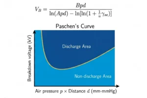
Where VB is the breakdown voltage, p is pressure, and d is the gap distance, is the secondary-electron-emission coefficient, A is the saturation ionization in the gas at a particular E/p (Electric field/pressure), and B is related to the excitation and ionization energies. A modern power tester must not only provide the voltage but also manage the automation of this pressurized environment, monitoring sensors in real-time to ensure the “atmospheric insulation” is active before the first pulse is fired.
Dynamic Testing: The New Frontier at Wafer Sort
The real breakthrough in modern wafer testing is the integration of specialized circuitry to perform tests that were previously only possible on packaged parts.
Reverse Recovery Time (Trr) and Triac Testing
For power diodes and MOSFET body diodes, the Reverse Recovery Time (Trr) is a critical parameter for switching efficiency. Measuring this at the wafer level requires dedicated, high-speed switching circuits integrated directly into the load board to minimize the inductive loop. Similarly, for AC applications, the predisposition for Triac testing allows for the characterization of bidirectional thyristors in their native wafer state, ensuring that the triggering and holding currents meet specifications before the die is integrated into complex power modules.
Unclamped Inductive Switching (UIS) and Avalanche
Perhaps the most stressful test for a power device is the UIS test, which simulates the energy a device must dissipate when switching an inductive load. Performing this on a wafer requires the tester to manage significant energy pulses. Modern load boards now include a matrix of integrated coils allowing for 100% avalanche testing on the wafer. This ensures that any crystal lattice defects that might lead to an avalanche failure are caught early.
Gate Integrity and Rgate Characterization
For SiC MOSFETs, the gate oxide is the “Achilles’ heel.” Traditional testers often overlook the internal gate resistance (Rg). By integrating a matrix to multiplex LCR meter resources directly on the load board, manufacturers can perform precise Rgate tests across multiple sites. This, combined with high-speed gate drivers capable of 16 programmable RGate ON/OFF values, allows for a perfect emulation of the final application’s switching behavior.
Advanced Protection: Safeguarding the Silicon
Testing at 128A and 3500V on a wafer is an exercise in controlled “violence” against the silicon. Without advanced protection, the equipment becomes a liability.
Run-Time Spike Detection
During the high-speed switching of SiC devices, parasitic inductances can cause voltage spikes on the Gate-Source junction. Even a microsecond spike exceeding 40V can cause “soft damage” to the gate oxide, leading to failure months later in the field.
Innovative testers now feature Run-Time Spike Detectors that actively monitor the Vgs during the entire test sequence. If a spike exceeds user-defined thresholds, the die is failed and binned for analysis. This is not just a test; it’s a safeguard for long-term reliability.
Overcurrent Protection and Needle Balancing
The probe needles are the weakest link in the high-current path. If 100A is not perfectly distributed across the contact needles, “needle melt” can occur. Dedicated Overcurrent Protection Modules are now used to balance the current between needle groups. This hardware-level protection limits the current based on the physical carry-capacity of the needles, preventing catastrophic damage to the wafer and reducing the total cost of ownership by extending probe card life.
Precision in the Nano-Scale: Low Current Measures
While the “Power” side of the tester handles the Amps, the “Analog” side must handle the Pico-Amps. Measuring leakage current (Idss) with 100pA resolution at the wafer level is notoriously difficult due to factory floor noise.
The use of Pico-Ampere Meter modules directly on the DUT board—rather than inside the tester cabinet—minimizes the connection length. This “localized” measurement avoids the noise inherent in long cable runs and provides the accuracy required for the most stringent automotive leakage specs.
The Next Level: Dual-Side Probing and “Virtual KGD Testing”
As power device architectures evolve, a new challenge has emerged: Double-Sided Dies. Many modern power semiconductors utilize the top surface for control circuitry and the bottom surface for high-current paths. Traditional probers, which rely on a solid chuck to contact the back of the wafer, face a significant limitation: the Chuck Resistance.
In a standard setup, the electrical path travels through the chuck, whose resistance can fluctuate depending on the position of the die on the wafer. This variability makes it nearly impossible to achieve the extreme accuracy required for Kelvin tests or RDSon measurements.
Eliminating Chuck Influence
To overcome this, Dual-Side Probing has emerged as a transformative solution. By integrating independent probing units above and below the wafer, synchronized to the same die, the system can contact the device from both sides simultaneously.
This architecture provides two game-changing advantages:
- Identical Current Paths: Because the current travels through a couple of probes (top and bottom) rather than the chuck, the path length and resistance remain identical for every single die on the wafer.
- Extreme Accuracy in RDSon: This setup eliminates the parasitic variables of the prober hardware, allowing for incredibly precise resistance measurements, including Dynamic RDSon.
This capability effectively enables a “Virtual KGD Test.” By executing these challenging measurements at the wafer level with packaged-level precision, manufacturers can guarantee die performance with such high confidence that post-packaging characterization encounters much less defectiveness.
Parallelism and Throughput: The Multi-Site Advantage
Testing at the wafer level is only economically viable if it can match the throughput of the manufacturing line. This requires Multi-Site Parallelism.
Modern architectures allow for up to 32 or 64 sites to be tested in parallel. However, “parallel” doesn’t just mean “simultaneous.” It means that each site must have its own 4-quadrant instrumentation to ensure that a failure on Site 1 does not affect the measurement on Site 32.
Furthermore, the software environment must provide Real-time Production Monitoring for binning and yield analysis, and Customized Datalogging to track the “pedigree” of every die from its position on the wafer.
Conclusion: The New Standard for Power Wafer Sort
The era of simple “DC-only” wafer testing is coming to an end. As power semiconductors become more critical to global infrastructure, the ability to perform Dynamic AC tests, UIS, and high-precision dual-side characterization directly at the wafer level is becoming the industry standard.
By integrating power instrumentation, pressurized arcing suppression, and synchronized dual-side contact into a single platform, manufacturers can achieve something that was once considered impossible: a complete, packaged-grade characterization of a power device while it is still part of the wafer. This doesn’t just save money on packaging — it ensures that only the most robust, high-performance silicon moves forward to power the world.